

Singxer
Free Shipping to
Estimated delivery on
受取状況を読み込めませんでした
Brand Name: Singxer
Certification: NONE
Origin: CN(Origin)
Maximum Power Per Channel: NO POWER
Model Number: C-1
Package: Yes
Description:
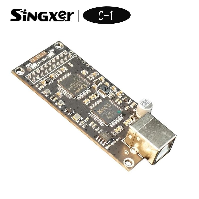
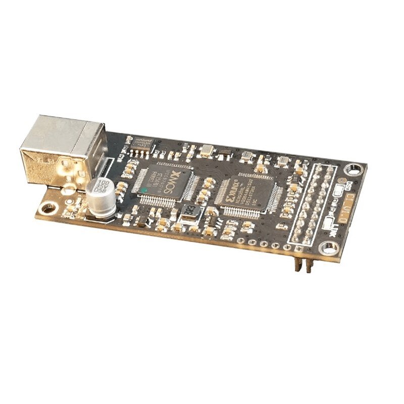
C-1 is our team developed a high-performance digital interface USB digital audio interface,adopted the latest XMOS xCORE - 200 series chips.C-1 is a low jitter clock system of digital interface.C-1 digital interface with a standard usb input interface,and F-1 has a lot of output interface,including I2S interface.
Technical Features:
1.C-1 is a the XMOS latest xCORE - 200 series of high-end products USB digital interface.A new generation of XMOS chip,using the more advanced process technology,the performance than the old one U8 chip doubled,the processing capacity of up to 1000 MIPS. 2.It is well known that the weight of the core of the digital audio is algorithm.Our team work in the field of digital audio for many years,at the same time get XMOS detailed FAE team's strong support,we are on the basis of the original firmware had done many of the technical improvement and optimization algorithm.
Technical indicators:
Each output interface to support the sampling rate of: PCM:44.1KHz,48KHz,88.2KHz,96KHz, 176.4KHz,192KHz,352.8KHz,384KHz DSD: 2.8 MHz (DSD64) - DoP,native 5.6 MHz (DSD128) - DoP,native 11.2 MHz (DSD256) - DOP,native A wide:top 32 bit over I2S output The highest bit over 24 S/PDIF Screw I2S row needle position is fully compatible with Italian Amanero module;The whole plate adopts the design of the three crystals,including audio crystals for customised version FeiMiaoJi crystals,SMT packaging small volume.
Each interface electrical standards:
1.USB input socket for standard USB - type B mother,USB power supply range is 4.5 V to 4.5 V; 2,.RCA S/PDIF signal output interface standard,level of 550 mv(standard load),the output impedance of 75 ohms.
Design details:
1.Electricity is the mother of the sound implementation of the design concept,attaches great importance to the power circuit design,USES the high performance,low noise and has fast response "as the main power supply.Whole board USES two-way independent power supply, "the clock part they even adopted the ADI ultra low noise, in order to ensure the output performance has laid a solid foundation to the extreme 2.PCB board USES 4 layer PCB design,make sure you have complete ground plane and the power supply layer,adopting high speed digital design method, ensure the whole signal integrity and power integrity.The clock signal for special processing,using the impedance of the package design and precise control,so as to ensure the quality of the clock signal and improve its anti-interference ability.Input and output signals are all follow the standard design,especially the USB high speed signal using the 90 ohms difference impedance control.
System compatibility:
1.Windows XP, Windows 7,Windows 8,Windows 10; 32/64 bit 2.Native MacOS 10.6 and later,use driver of your system 3.Native Linux with UAC2 compliant kernel,use driver of your system 4.Android OS 4.2 and upper,need device support OTG,and Android 5.0 is default,please use suitable player if below Android 5.0
I2S socket output signal instruction:
1.High electrical level MUTE,DSD ON is DSD date streams when high electrical level. 2.All electrical levels are LVCMOS,voltage is 3.3V. 3.3.3+ is output power supply,and output electric current is lower than 50mA. 4.MCLK output is 22.5792Mhz or 24.576Mhz clock. 5.FS0,FS1,FS2 is sampling rate indicate electricity level,FS3 not.
Worldwide Free Shipping on Hificat, Please allow 1-3 business days for conduct Quality Control in order to ensure the products quality.
In the event that a shipment is refused delivery by the recipient, is undeliverable, or is returned to sender, Hificat will process a refund to the original payment method used.
If a customer would like the order reshipped, they’ll be charged a reshipment fee. Customers may also be subject to a restocking fee of up to 20 percent of the product cost.
--------------------------------------------------------------------------------------
We collaborate with these courier companies:
Standard Shipping: Yanwen Express
Express Shipping(over $500 can be free): DHL Express, FedEx and SF Express
Hificat has extensive global logistics experience to ensure quality logistics services to consumers.
HiFiCat offers consumers different shipping, depending on the country, a choice of different shipping methods.
--------------------------------------------------------------------------------------
All taxes and duties are prepaid to the carrier by HiFiCat prior to shipping, so there are no taxes or duties to pay when you receive it. 6-10 days to arrive.
Tracking Example
France: https://t.17track.net/en#nums=YT2132021222003141
Germany: https://t.17track.net/en#nums=YT2133621222016083
United Kingdom: https://www.17track.net/?nums=GV779664269GB
Italy:https://t.17track.net/en#nums=YT2133021222011717
Spain:https://t.17track.net/en#nums=YT2129521222003430
United States:https://t.17track.net/en#nums=SUA211205BIUQ1000007
2.EU Country:Filand, Poland, Estonia, Norway, Switzerland, Greece, Sweden, Israel, Czech Republic, Slovenia, Slovakia, Denmark, Netherlands, Latvia, Croatia, Austria, Hungary, Belgium, Bulgaria, Romania, Ireland, Malta, Iceland, Serbia and so on.
All taxes and duties are prepaid to the carrier by HiFiCat prior to shipping, so there are no taxes or duties to pay when you receive it. 10-15 days to arrive.
Filand: https://www.17track.net/?nums=UG324191515YP
Poland: https://www.17track.net/?nums=UG335827360YP
Estonia: https://www.17track.net/?nums=UG363043181YP
Norway: https://www.17track.net/?nums=VR457380806YP
Switzerland: https://www.17track.net/?nums=UG359525911YP
Greece: https://www.17track.net/?nums=UG250851788YP
Sweden: https://www.17track.net/?nums=UG353458343YP
Israel: https://www.17track.net/?nums=UG356134837YP
Czech Republic: https://www.17track.net/?nums=UG320437102YP
Slovenia: https://www.17track.net/?nums=UG349882511YP
Slovakia: https://www.17track.net/?nums=UG349946557YP
Denmark: https://www.17track.net/?nums=UG272480001YP
Netherlands: https://www.17track.net/?nums=UG206078468YP
Latvia: https://www.17track.net/?nums=UG336264373YP
Croatia: https://www.17track.net/?nums=UG331204789YP
Austria: https://www.17track.net/?nums=UG322443180YP
Hungary: https://www.17track.net/?nums=UG313846849YP
Belgium: https://www.17track.net/?nums=UG313858025YP
Bulgaria: https://www.17track.net/?nums=UG309182635YP
Romania: https://www.17track.net/?nums=UG295530616YP
Ireland: https://www.17track.net/?nums=UG286654665YP
Malta:
Iceland: https://www.17track.net/?nums=VR447888050YP
Serbia: https://www.17track.net/?nums=VR447710777YP
Ukraine: https://www.17track.net/?nums=UG331240667YP
Russian Federation: https://www.17track.net/?nums=VR454415418YP
3.South America:Peru, Brazil, Chile
Chile: https://www.17track.net/?nums=UG205949999YP
Brazil: https://www.17track.net/?nums=UG207476109YP
New Zealand: https://www.17track.net/?nums=YE175499582CN
5.Canada By Canada Post, about 2 weeks.

