

Singxer
Free Shipping to
Estimated delivery on
Canada, Mexico, Romania, United States: import duty of 10 USD
Couldn't load pickup availability
Brand Name: Singxer
Certification: NONE
Origin: CN(Origin)
Maximum Power Per Channel: NO POWER
Model Number: SU-2
Package: Yes
Channels: 2 (2.0)
Product Description:
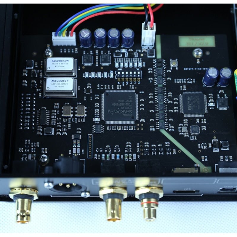
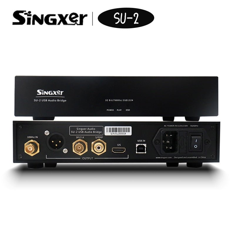
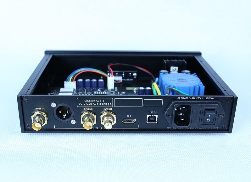
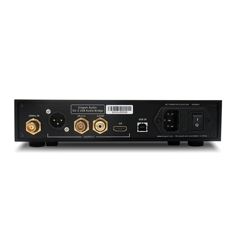
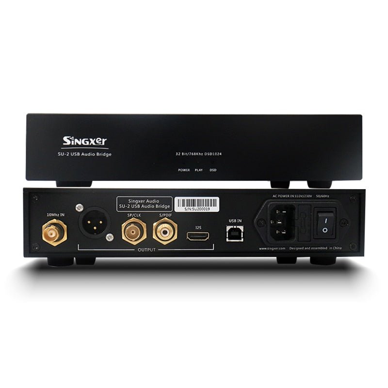
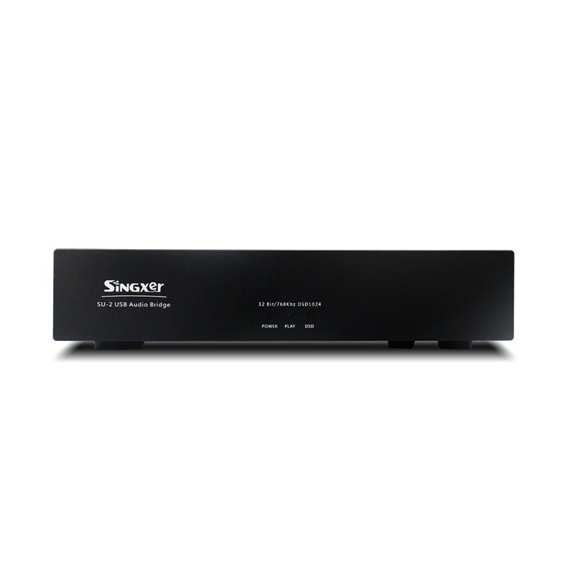
The SU-2 digital interface is a high-performance USB digital audio interface. The microprocessor with the latest ARM Cortex-M4 as the core is used as the main control of the USB data part. SU-2 uses a self-developed ultra-low jitter clock system (ACCUSILICON's AS-318B series, which achieves ultra-low jitter at the femtosecond level). A large-capacity FPGA serves as the digital audio data processing core and has a standard USB2.0 input interface. Rich output interface, including XLR balanced output AES, coaxial RCA and BNC, I2S interface with HDMI socket output, perfect master clock and word clock (WCLK) output. SU-2 supports external 10Mhz clock input, using common 50 ohm input impedance design.
The SU-2 is not only a USB interface, it can also be used as an independent master clock product.
1. When used as an independent master clock, it can output a word clock of 44.1K-384K, or output a master clock of 22.5792Mhz-49.152Mhz. (When not connected to USB, it will be used as the master clock device by default)
2. When using an external 10Mhz clock input, it can also be used as a frequency converter; support 10Mhz to 44.1K-384K word clock, or output 22.5792Mhz-49.152Mhz master clock.
SU-2 is a new architecture USB interface developed by us to replace the original SU-1; PCM sampling rate supports up to PCM 768K, and DSD supports up to DSD1024. Using a large FPGA as the core of the processing processing, we decentralized some of the FPGA algorithm technology of the flagship interface SU-6 to the SU-2; its positioning in the mid-to-high-end interface mainly uses the following three unique technologies:
1. Full isolation technology (ground isolation), using 150Mbps full isolation chip, can completely isolate the interference from the PC;
2. Source synchronization technology and FPGA shaping technology, reshape the I2S signal after isolation; thus eliminating the additive jitter brought by the isolation chip;
3. Self-developed clock system, using ACCUSILICON high-performance crystal oscillator, low phase noise, low jitter; you can also choose external 10Mhz clock, support various atomic clocks, constant temperature crystal, GPDSO input.
This product supports two kinds of AC power voltage, 230V and 115V respectively. Please choose the volts suitable for your country's voltage.
The driver was updated in June 2019. The latest version is V4.67. The latest driver supports DSD1024 and DSD NATIVE modes.
Technical indicators:
Sampling rates supported by each output interface:
PCM: 44.1KHz, 48KHz, 88.2KHz, 96KHz,
176.4KHz, 192KHz, 352.8KHz, 384KHz, 705.6KHz, 768KHz
[Where I2S out supports all sampling rates, S / PDIF supports up to 384KHz, DOP128]
2.8 MHz (DSD64)-DOP, native
5.6 MHz (DSD128)-DOP, native
11.2 MHz (DSD256)-DOP, native
22.5792 MHz (DSD512)-DOP, native
45.1584 MHz (DSD1024)-native
[Which I2S out supports all DSD formats, S / PDIF and AES / EBU support DSD128 DOP mode]
Bit width: up to 32 bit over I2S output
24 bit over S / PDIF
Electrical standards for each interface:
1. The USB input socket is a standard USB-B female socket, and the USB power supply range is 4.5V-5.1V;
2. The RCA interface outputs standard S / PDIF signals with a level of 550mV (connected to a standard load) and an output impedance of 75 ohms;
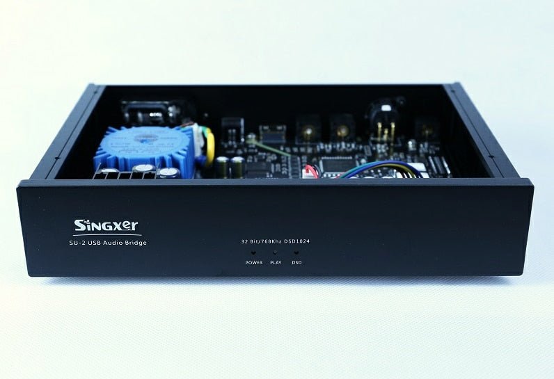
3. The power input is 115V / 230V AC, and the internally imported transformer is used for power supply.
Details:
1. We attach great importance to the design of power supply circuits, using LDOs with high performance, low noise and fast response as the main power supply. The entire board uses multiple independent LDO power supplies, and the clock part even uses ADI's ultra-low noise LDO, which lays a solid foundation for ensuring the ultimate output performance.
2. The PCB main board adopts a 4-layer circuit board design to ensure a complete ground plane and power layer. A high-speed digital design method is used to ensure the signal integrity and power integrity of the entire board. The clock signal is specially processed, and the grounded design and precise impedance control are adopted to ensure the clock signal quality and improve its anti-interference ability. The input and output signals follow the standard design, especially the USB high-speed signals use 90 ohm differential impedance control.
System compatibility:
1, Windows 7, Windows 8, Windows 10; 32/64 bit, special drivers need to be installed
2, Native MacOS 10.6 and later, using the system's own driver
3.Native Linux with UAC2 compliant kernel, using the system's own driver, (tested on Ubuntu and Daphile systems, based on INTEL X86 platform)
4, Android OS 4.2 and above, the device needs to support the OTG function. Generally speaking, Android 9.0 and above systems are supported by default. It is recommended to use it with specialized players below 9.0.
I2S interface uses HDMI socket output:
1. 3.3V LVDS differential signal;
2. DSD ON signal, 5V power supply (small current), CPLD has been processed inside the MUTE signal, and there is no need to output the MUTE signal;
3. The DSD ON signal can be defined by itself. The DSD ON signal can be arbitrarily output to the PIN 13, 14, 15, 16 pins of the socket.
Flexible I2S and clock output configuration:
1. Switches 1-4 correspond to the PIN13-16 pins of the HDMI socket. Pull to the ON position, it means that the HDMI PIN has the function of DSD_ON.
2. Switches 5 and 6 are the modes that configure the clock output:
When the switch 5 is OFF, the clock outputs MCLK, and when it is ON, the clock outputs WCK.
Switch 6 configures the frequency of MCLK, which is 22.5792M / 24.576M when OFF, and 45.1584M / 49.152M when ON;
The configuration of switch 6 is valid for CLK OUT, RJ45-I2S, and HDMI-I2S.
3. Switch 7 can set the left and right channels in DSD mode in I2S signal separately.
4. Switch 8 can set the BCLK line sequence in the I2S signal; when OFF, PIN4 is BCLK + and PIN6 is BCLK-;
5. Switch 9 can set the line sequence of LRCLK in I2S signal; when OFF, PIN7 is LRCLK + and PIN9 is LRCLK-;
6. Switch 10 can set the line sequence of DATA in I2S signal; when OFF, PIN1 is DATA + and PIN3 is DATA-;
The SU-2 can be configured via SW switches to suit different I2S standards.
However, as far as we know, HDMI-I2S is different for every manufacturer in the world. For most manufacturers, HDMI-I2S is a proprietary protocol of the manufacturer. Therefore, I'm sorry, SU-2 cannot adapt to all HDMI-I2S machines, so we cannot accept returns due to incompatible I2S interfaces.
Case size and packaging:
Case L*W*H: 234MM * 170MM * 46MM, excluding the height of the feet and the protruding part of the connector on the back of the case.
Stand-alone weight: 1.8KG.
L*W*H of carton package: 350MM * 230MM * 110MM.
Shipping package weight: 2.3KG
Accessories: a USB cable and a power cable.
Worldwide Free Shipping on Hificat, Please allow 1-3 business days for conduct Quality Control in order to ensure the products quality.
In the event that a shipment is refused delivery by the recipient, is undeliverable, or is returned to sender, Hificat will process a refund to the original payment method used.
If a customer would like the order reshipped, they’ll be charged a reshipment fee. Customers may also be subject to a restocking fee of up to 20 percent of the product cost.
--------------------------------------------------------------------------------------
We collaborate with these courier companies:
Standard Shipping: Yanwen Express
Express Shipping(over $500 can be free): DHL Express, FedEx and SF Express
Hificat has extensive global logistics experience to ensure quality logistics services to consumers.
HiFiCat offers consumers different shipping, depending on the country, a choice of different shipping methods.
--------------------------------------------------------------------------------------
All taxes and duties are prepaid to the carrier by HiFiCat prior to shipping, so there are no taxes or duties to pay when you receive it. 6-10 days to arrive.
Tracking Example
France: https://t.17track.net/en#nums=YT2132021222003141
Germany: https://t.17track.net/en#nums=YT2133621222016083
United Kingdom: https://www.17track.net/?nums=GV779664269GB
Italy:https://t.17track.net/en#nums=YT2133021222011717
Spain:https://t.17track.net/en#nums=YT2129521222003430
United States:https://t.17track.net/en#nums=SUA211205BIUQ1000007
2.EU Country:Filand, Poland, Estonia, Norway, Switzerland, Greece, Sweden, Israel, Czech Republic, Slovenia, Slovakia, Denmark, Netherlands, Latvia, Croatia, Austria, Hungary, Belgium, Bulgaria, Romania, Ireland, Malta, Iceland, Serbia and so on.
All taxes and duties are prepaid to the carrier by HiFiCat prior to shipping, so there are no taxes or duties to pay when you receive it. 10-15 days to arrive.
Filand: https://www.17track.net/?nums=UG324191515YP
Poland: https://www.17track.net/?nums=UG335827360YP
Estonia: https://www.17track.net/?nums=UG363043181YP
Norway: https://www.17track.net/?nums=VR457380806YP
Switzerland: https://www.17track.net/?nums=UG359525911YP
Greece: https://www.17track.net/?nums=UG250851788YP
Sweden: https://www.17track.net/?nums=UG353458343YP
Israel: https://www.17track.net/?nums=UG356134837YP
Czech Republic: https://www.17track.net/?nums=UG320437102YP
Slovenia: https://www.17track.net/?nums=UG349882511YP
Slovakia: https://www.17track.net/?nums=UG349946557YP
Denmark: https://www.17track.net/?nums=UG272480001YP
Netherlands: https://www.17track.net/?nums=UG206078468YP
Latvia: https://www.17track.net/?nums=UG336264373YP
Croatia: https://www.17track.net/?nums=UG331204789YP
Austria: https://www.17track.net/?nums=UG322443180YP
Hungary: https://www.17track.net/?nums=UG313846849YP
Belgium: https://www.17track.net/?nums=UG313858025YP
Bulgaria: https://www.17track.net/?nums=UG309182635YP
Romania: https://www.17track.net/?nums=UG295530616YP
Ireland: https://www.17track.net/?nums=UG286654665YP
Malta:
Iceland: https://www.17track.net/?nums=VR447888050YP
Serbia: https://www.17track.net/?nums=VR447710777YP
Ukraine: https://www.17track.net/?nums=UG331240667YP
Russian Federation: https://www.17track.net/?nums=VR454415418YP
3.South America:Peru, Brazil, Chile
Chile: https://www.17track.net/?nums=UG205949999YP
Brazil: https://www.17track.net/?nums=UG207476109YP
New Zealand: https://www.17track.net/?nums=YE175499582CN
5.Canada By Canada Post, about 2 weeks.


